If the future were to be categorized in one word, it would be "data-centric". For decades, IC vendors have designed chips that have all functions integrated on the same die; however, scaling monolithic IC becomes more difficult and costly as the industry sees the slowdown of Moore's law. IC vendors have been pushed towards "advanced semiconductor packaging" to meet the world's data needs.
Today, there is an explosion of data at every level and in almost every industry. Every second, the digital world generates 4,000 terabytes of data, and this amount is only expected to go considerably up in the future. Data-rich applications such as machine learning and AI are the key data enablers in a wide range of applications, including data centers, 5G, and autonomous vehicles. A powerful processor is required to run these apps, of which the foundation is an integrated circuit (IC) built on Si.
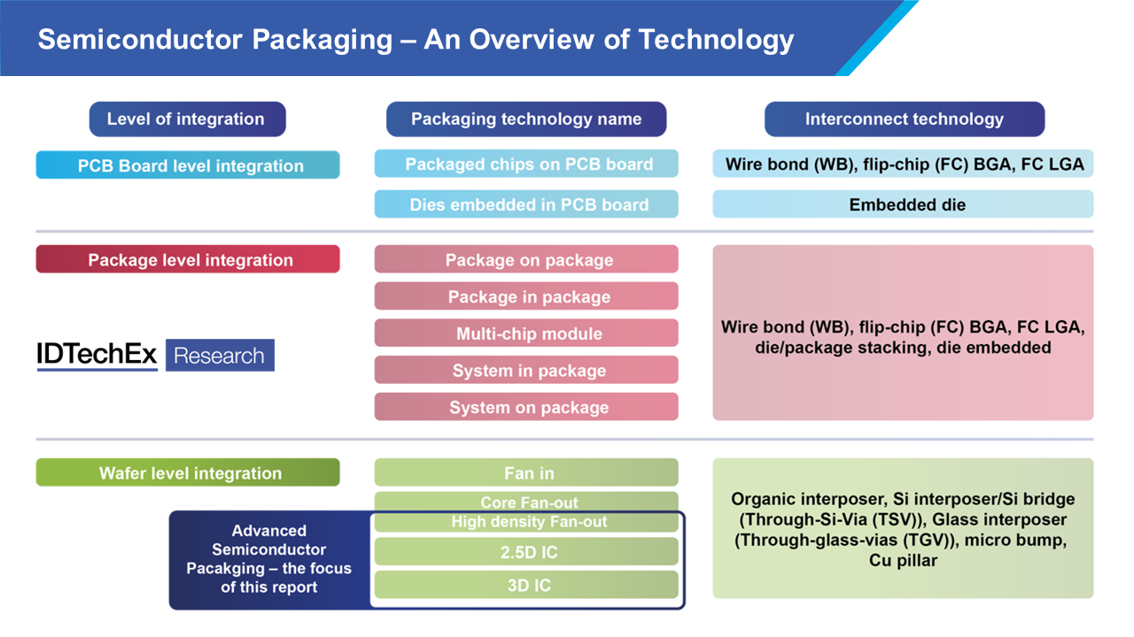
What is advanced semiconductor packaging?

Source: IDTechEx - "Advanced Semiconductor Packaging 2023-2033"
The semiconductor packaging process plays a key role in semiconductor manufacturing and design. For example, in the IC packaging process, the IC bare die is encapsulated in a supporting case with electrical contacts. The casing protects the IC bare die from physical harm and corrosion and links the IC to a PCB board to other devices. Semiconductor packaging has existed for decades - the first volume production of semiconductor packaging came in in the early 1970s. So, what is new?
As mentioned, due to the slowdown of Moore's law and the increasing cost of manufacturing a monolithic IC, vendors required new design approaches to enable high-performance, cost-effective processors. A new design called a "chiplet" is the key trend going forwards.
The idea behind chiplets is to "split" a monolithic IC into multiple functional blocks, reconstitute the functional blocks into separate chiplets, and then "re-assemble" these at the package level. Ideally, a processor based on chiplet design should have the same or greater performance but lower total production cost than a monolithic IC. Packaging methods, particularly those used to link several chiplets, play a crucial role in chiplet design since they affect the system's performance as a whole. These packaging technologies, including 2.5D IC, 3D IC, and high-density fanout wafer level packaging, are categorized as "advanced semiconductor packaging" and are the subject of IDTechEx's newly released research report "Advanced Semiconductor Packaging 2023-2033". They allow for the merging of multiple chiplets at various process nodes on a single substrate and have small bump sizes to enable higher interconnect densities and higher integration capabilities.
The brand new IDTechEx report includes a detailed examination of the latest innovations in advanced semiconductor packaging technology, key technical trends, analysis across the value chain, major player analysis, and granular market forecasts. Furthermore, this study gives a comprehensive evaluation of the semiconductor industry in general.
Advanced semiconductor packaging serves as a critical foundation for next-generation ICs that will be utilized in four key markets: data centers, 5G, autonomous vehicles, and consumer electronics. IDTechEx leverages its expertise in these sectors to provide the reader with a thorough understanding of how advanced semiconductor packaging is influencing these fields and what the future may hold.
For a further understanding of the overall advanced semiconductor packaging markets, players, technologies, opportunities, and challenges, please refer to the IDTechEx report "Advanced Semiconductor Packaging 2023-2033".
For more information on this report, please visit www.IDTechEx.com/ASP or for the full portfolio of research available from IDTechEx please visit www.IDTechEx.com.
IDTechEx guides your strategic business decisions through its Research, Subscription and Consultancy products, helping you profit from emerging technologies. For more information, contact research@IDTechEx.com or visit www.IDTechEx.com.


