

As semiconductor packaging technologies evolve, 2.5D packaging and 3D Cu-Cu hybrid bonding are becoming essential routes to higher performance and improved power efficiency. However, manufacturing these packages at high yield requires careful material selection, process control, and continued innovation in packaging manufacturing techniques. IDTechEx's latest report, "Materials and Processing for Advanced Semiconductor Packaging 2027-2037: Technologies, Players, Forecasts," examines these challenges across 2.5D packaging materials and process flows, including silicon, organic-based materials, and glass, as well as Cu-Cu hybrid bonding for 3D integration. The report also provides 10-year forecasts for organic dielectric and glass-based advanced semiconductor packaging modules, covering both unit and area projections.
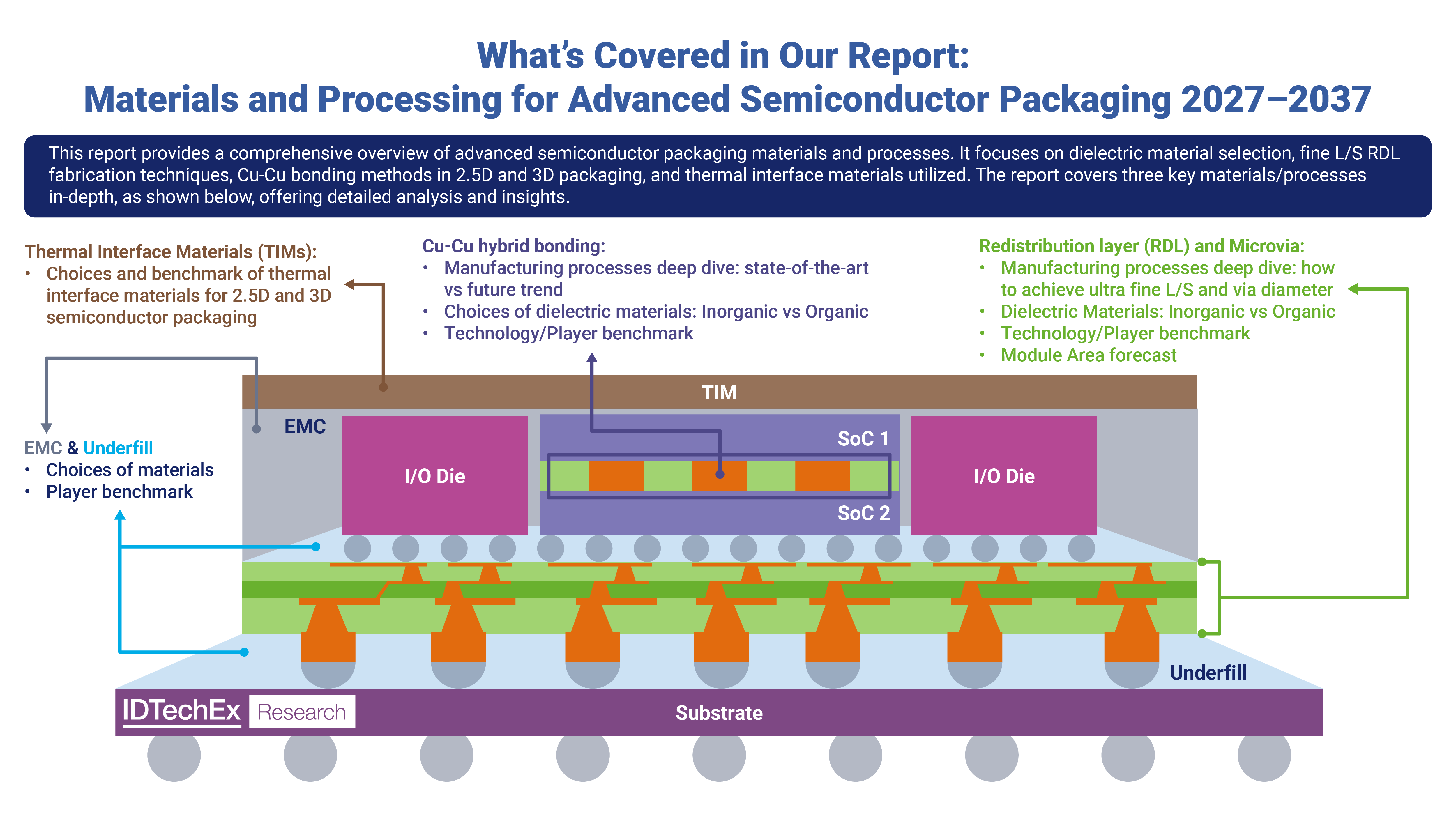
Source: IDTechEx report Materials and Processing for Advanced Semiconductor Packaging 2027-2037: Technologies, Players, Forecasts
2.5D interposer materials:
In 2.5D packaging, different chiplets are interconnected horizontally through interposers, with three main materials are being considered: silicon (Si), organic, and glass. Silicon interposers are the industry standard for high-performance computing (HPC) due to their ability to support fine routing, but their high cost and packaging area limitations are challenges. To mitigate these, localized Si bridges are the next step forward. Organic interposers offer a cost-effective alternative, particularly through Fan-Out Panel Level Packaging (FOPLP), which increases area utilization and lowers costs by up to 60%. However, achieving fine routing similar to silicon remains difficult.
Glass interposers/Glass Core Substrates (GCS), has the potential to support fine routing density, provide good dimensional stability, reduce warpage in large-area packages, offer tunable coefficient of thermal expansion, enable low-loss electrical performance, and so on. Importantly, glass is also compatible with panel-level processing, which makes it attractive as package sizes continue to increase for AI/HPC chips. However, several manufacturing challenges remain, including process control and yield improvement in through-glass via formation and metallization, large-panel handling, glass cracking and mechanical reliability issues, cleanliness and contamination control, and so on. Mitigating failures in glass substrates requires design-, material-, and process-level optimization rather than a single-point solution. Therefore, while glass offers strong potential as a scalable material platform, its adoption will depend on whether the manufacturing ecosystem can address these manufacturing challenges at high volume.
Overall, as the ecosystem evolves, each material brings its own strengths and challenges to 2.5D packaging, with a focus on balancing performance, scalabulity, and cost.
Cu-Cu hybrid bonding manufacturing:
Wafer-to-Wafer (W2W) and Die-to-Wafer (D2W) hybrid bonding are two key approaches for 3D hybrid bonding, each with distinct advantages and challenges. W2W bonding, the more established process, involves bonding two full wafers, typically in a single, uniform step. This approach benefits from consistent surface area, making alignment and bonding relatively straightforward. With wafers always maintaining a round shape, the process can be optimized for high throughput, making it suitable for large-scale production. However, W2W bonding is less flexible in handling different chip sizes and is limited by the need to bond identical wafers.
On the other hand, D2W hybrid bonding is more complex and addresses the limitations of W2W when dealing with high-performance dies of different sizes. Instead of bonding entire wafers, D2W involves the precise bonding of individual dies onto a target wafer, enabling the integration of different die sizes and types in a single package. This flexibility makes D2W bonding ideal for advanced packaging techniques like chiplet integration, allowing manufacturers to mix and match dies with different functions. However, D2W presents significant manufacturing challenges. D2W demands ultra-clean, particle-free surfaces and precise alignment, as any contamination or misalignment can lead to defects, significantly compromising bonding qualities.
Additionally, D2W bonding introduces complications with die aspect ratios. Dies with higher aspect ratios can cause unilateral bonding issues, where the bond front starts along one side, potentially leading to a scaling effect. The use of flexible organic carriers or adhesives during dicing further complicates the process. Moreover, D2W bonding is more sensitive to queue times, which can degrade surface quality before bonding occurs.
Despite these challenges, D2W bonding's flexibility and precision are increasingly critical for high-performance applications, while integrated hybrid bonding tools are emerging to address many of these hurdles.
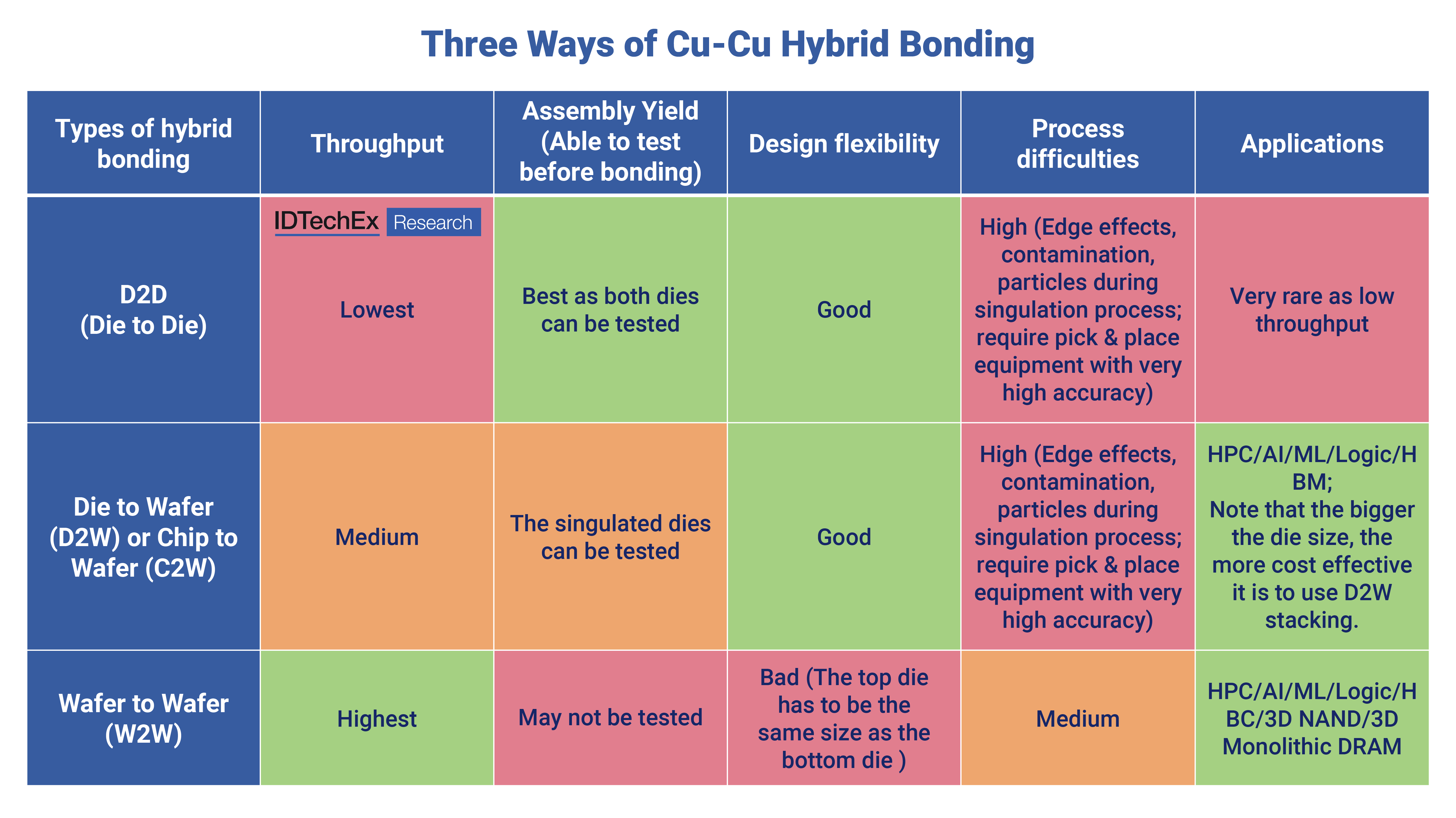
Three ways of Cu-Cu hybrid bonding. Source: IDTechEx report Materials and Processing for Advanced Semiconductor Packaging 2027-2037: Technologies, Players, Forecasts
Thermal Interface Materials for next generation advanced semiconductor packaging:
Thermal management is also a critical material consideration in advanced semiconductor packaging. In 2.5D packages, high-power logic dies and HBM stacks are placed side by side under the same heat spreader, increasing total package power and creating local hot spots. In 3D packaging, the challenge becomes more severe, as vertically stacked dies can create buried heat sources with limited heat removal pathways.
This is increasing the importance of thermal interface materials for 2.5D and 3D packaging. TIM selection is driven by several factors, including thermal resistance, material thermal conductivity, mechanical reliability, contact quality, ease of testing, cost, and compatibility with high-volume manufacturing. Different TIM1 and TIM1.5 solutions are being explored, including polymer-based thermal greases, solid metal TIMs such as indium foils, liquid metals, and graphene-based materials. IDTechEx's report examines the potential roadmap for TIMs in advanced semiconductor packaging, key material selection considerations, candidate materials, and relevant case studies.
What is covered in IDTechEx's latest Materials and Processing for Advanced Semiconductor Packaging 2027-2037: Technologies, Players, Forecasts report
The report begins by outlining the key technology drivers behind 2.5D and 3D packaging adoption, before examining the materials and process flows required to support next-generation package architectures. A core chapter focuses on 2.5D packaging, including RDL formation, microvia fabrication, interconnect scaling, and dielectric material selection. It covers both inorganic platforms such as silicon and glass, as well as organic dielectric materials used in RDL and substrate-level integration. The report also assesses epoxy mold compounds (EMC) and mold underfill (MUF), where thermal, mechanical, and reliability requirements are becoming increasingly important.
A major update in this edition is the addition of a dedicated section of approximately 70 slides on glass panel-based advanced semiconductor packaging. This section analyzes glass substrates and glass interposers, covering technology roadmaps, manufacturing processes, key technical challenges, development directions, supply chain activities, company profiles, and the future outlook for glass-based packaging.
"Materials and Processing for Advanced Semiconductor Packaging 2027-2037: Technologies, Players, Forecasts" also includes a dedicated chapter on Cu-Cu hybrid bonding for 3D die stacking. It examines manufacturing processes, bonding equipment, material requirements, and case studies using both organic and inorganic dielectrics. This edition places greater emphasis on low-temperature and room-temperature Cu-Cu hybrid bonding, reflecting growing industry interest in reducing thermal budgets and enabling hybrid bonding across a wider range of devices and material platforms.
Another new addition is a section on thermal interface materials for 2.5D and 3D packaging. As advanced packages integrate multiple chiplets, HBM stacks, and vertically stacked components, thermal management is becoming a critical design constraint. This section discusses the potential roadmap for TIMs in semiconductor packaging, key material selection considerations, emerging candidates, and relevant case studies.
The report includes 10-year forecasts for organic dielectric and glass-based advanced semiconductor packaging modules, covering both unit shipments and total module area. The forecasts assess adoption across AI accelerators, server CPUs, ADAS chips in autonomous vehicles, and consumer electronics, especially highlighting the increasing importance of large-area advanced packaging platforms in AI and HPC applications.
For more information on this report, including downloadable sample pages, please visit www.IDTechEx.com/MatsforASP, or for the full portfolio of related research available from IDTechEx, see www.IDTechEx.com/Research/Semiconductors.
